- i2S and wishbone with the source code and everything
- i2S and LMMI IP
- Some documentation of a i2S transmitter
The frequency of operation in the eVolito is 102400
Modes of i2S
i2S can be generated in two ways: Master and slave (for the line-converter).
- Master it means that the line-converter (the A/D) generate the LRCK (word select clock) and the SCLK (bit clock i2s_sck), as subclocks of the master clock mclk. The master mode is know as Philips mode.
- Slave mode, all the clocks are generated outside the line-converter. The ratio of each clock is stated in the datasheet.
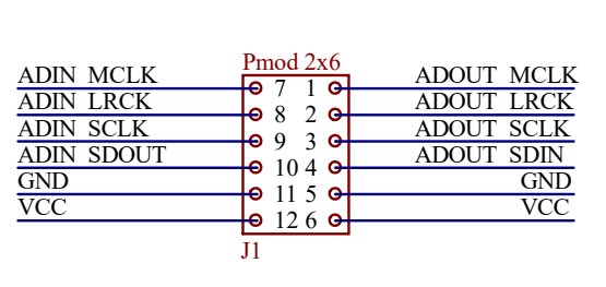
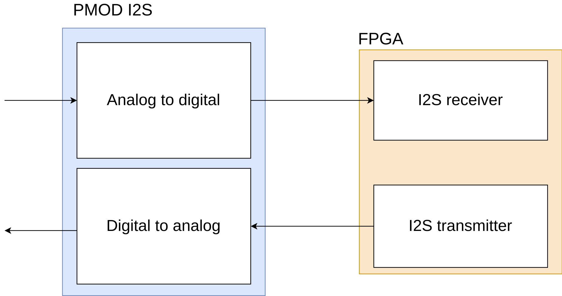
PMOD to i2S

Be careful becuase the name of the component is different from the stated in the IP of wishbone.
- mclk -> another high frequency clock that we need to generate in order everything to work.
- lrclk -> Is the word select pint, in the code is i2s_ws
- sclk -> is the bit clock, that is the i2s_sck
Some considerations of clocks in the i2s interface
From the library of I2S it is defined this equation to get the F_BCLK:
- Frequency BCLK = SampleRate x BitsPerChannel x numberOfChannels
From eVolito (defines.h ADC_*):
- SampleRate: 4000
- BitsPerChannel: 16. From 32 Bits per sample (adc.cpp line 24)
- NumberOfChannels: 2
$$ F_{BCLK} = 4000 \cdot 16 \cdot 2 = 128 \ KHz $$
The nomeclature is:
- SSM -> Single-Speed Mode
- DSM -> Double-Speed Mode
- QSM -> Quad-Speed Mode
The ratio MCLK/LRCK is the SCLK rate.
line-in converter = The Pmod I2S2 board.
Master Mode or Slave Mode by setting mode jumper JP1 to the corresponding position. In Slave Mode, LRCK and SCLK must be generated by the host board. In Master Mode, both LRCK and SCLK are automatically generated by the line-in converter.
THE WISHBONE i2S INTERFACE IS CONFIGURED TO WORK ONLY AS MASTER; SO IT IS VALID ONLY THE SLAVE MODE ON THE line-in converter (The pmod i2s board).
In the docs there is a nice description of the clocks frequency. Basically in the basic diagram of i2s normally is not described the master clock, but in some design is necessary to syncronize everything.
Line Out Serial Clock Generation
The SCLK (BCLK) is generated by the MCLK.
From eVolito:
- Master Mode is selected.
- MCLK -> 1.024 MHz (define.h) . This value came from the datasheet (CS5343), page 9, from the Single-Speed 256x max 977 ns.
- 32 Bits per sample (adc.cpp line 24)
- F_BCLK = 128 KHz, from the equation above.
Analog characteristics
The input signal is 0.568*VA Vpp. Where VA is 3.7V. For testing you can put a signal with 1.5Vpp
—
I2S Wishbone interface
I2s transmit testbench
Necessary to set:
constant DATA_WIDTH:integer:=16;
constant ADDR_WIDTH:integer:=6;
constant IS_RECEIVER:integer:=0;
And then, fix the length of 2 lines, that will appear as error.
Source, the testbench of the i2s to wishbone IP.
The steps are:
- store in registers of the left. Adress “1xxxxx” even
- store in registers of right. Adress “1xxxxx” odd.
- configure register: 4. 0011101010001011 5. TXEN - 1 6. TINTEN - 1 7. TSWAP - 0 8. MLSBF - 1 -> tx_int_o is active if the data in the lower half of the sample buffer has been transmitted by the i2s transmit master 9. MHSBF - 0 10. RES - 010100 (16) Adresses of length 16 11. RATIO - 00111 (7) -> i2s_sck_o = (50Mhz) / (2*(7+2)) = 2.78 MHz
Explanation. The tx_int_o is active 2 times, the first to say that the first part of the buffer was sent, and the second, that he second part of the buffer was sent, that is, the information was sent correclty.
First example, relay the input with the output
Clock of the FPGA 12 MHz. The output should be the same as is in the volito right now.
From eVolito (defines.h ADC_*):
-
SampleRate: 4000
-
BitsPerChannel: 16. From 32 Bits per sample (adc.cpp line 24)
-
NumberOfChannels: 2
-
Frequency BCLK (SCLK) = SampleRate x BitsPerChannel x numberOfChannels = 128 KHz
-
Is going to work at Single-Speed, 256x Mode
-
SCLK / LRCK = 64 => LRCP = 2 KHz
-
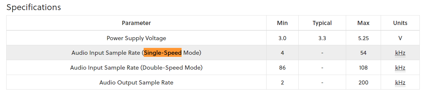
From the data sheet, in order to work on Single-Speed, 256x Mode, the min MCLK period is 72, and max is 976. The possible clock that is multiple of 256x, and follow the ratio of MCLK/LRCK 256x, is that MCLK is 2.048 MHz.
CLOCKS (FROM ABOVE):
- MCLK -> 2.048 MHz
- BCLK (SCLK) -> 128 KHz
- LRCK (Word select) -> 2 KHz
The previous clocks were not working, so I created this ones:
- Sample rate is 4 KHz => LRCK 4 KHz (1 / 64 SCLK)
- SCLK / LRCK = 64x => SCLK 256 KHz (1 / 4 MCLK)
- MCLK / LRCK = 256 => MCLK 1.024 MHz
EDIT 20230829: Now is working, it is the example under clock_generation. I am not able to decode yet, but is just understanding the settings.
To make this possible the tasks are:
- Create an example that the iCEBreaker is generating the necessary clocks
- Implement the clocks example on the FPGA
- Connect the FPGA to the digital signal analyser and see if I am able to receive i2S
- Create a transmiter of i2S with constant frequency
- Understand the receiver example
- Conect the receiver to the transmitter of i2S
Possible error
When the data width is set to 32 bits, the clocks seems to be for 16 bits. Interesting.This problem is because you need to define also the RES correctly on the 0x0 addres.